(China (Mainland))

Product Summary
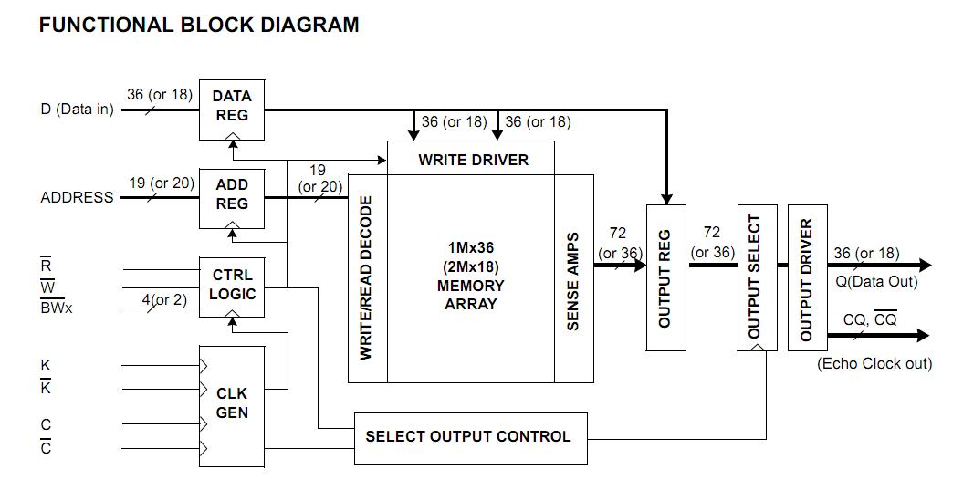
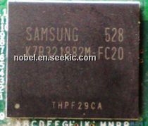
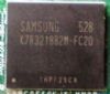
The K7R321882M-FC20 is a 37,748,736-bits QDR (Quad Data Rate) Synchronous Pipelined Burst SRAM. The device is organized as 1,048,576 words by 36bits for K7R323682C, 2,097,152 words by 18 bits for K7R321882C and 4,194,304 words by 9bits for K7R321882M-FC20. The K7R321882M-FC20 is implemented with SAMSUNG’s high performance 6T CMOS technology and is available in 165pin FBGA packages. Multiple power and ground pins minimize ground bounce.
Parametrics
K7R321882M-FC20 absolute maximum ratings: (1)Voltage on VDD Supply Relative to VSS, VDD: -0.5 to 2.9 V; (2)Voltage on VDDQ Supply Relative to VSS, VDDQ: -0.5 to VDD V; (3)Voltage on Input Pin Relative to VSS, VIN: -0.5 to VDD+0.3 V; (4)Storage Temperature, TSTG: -65 to 150℃; (5)Operating Temperature Commercial / Industrial, TOPR: 0 to 70 / -40 to 85℃; (6)Storage Temperature Range Under Bias, TBIAS: -10 to 85℃.
Features
K7R321882M-FC20 features: (1)1.8V+0.1V/-0.1V Power Supply; (2)DLL circuitry for wide output data valid window and future frequency scaling; (3)I/O Supply Voltage 1.5V+0.1V/-0.1V for 1.5V I/O, 1.8V+0.1V/-0.1V for 1.8V I/O; (4)Separate independent read and write data ports with concurrent read and write operation; (5)HSTL I/O; (6)Full data coherency, providing most current data; (7)Synchronous pipeline read with self timed early write; (8)Registered address, control and data input/output; (9)DDR (Double Data Rate) Interface on read and write ports; (10)Fixed 2-bit burst for both read and write operation; (11)Clock-stop supports to reduce current; (12)Two input clocks (K and K) for accurate DDR timing at clock rising edges only; (13)Two input clocks for output data (C and C) to minimize clock-skew and flight-time mismatches; (14)Two echo clocks (CQ and CQ) to enhance output data traceability.; (15)Single address bus; (16)Byte write function; (17)Separate read/write control pin (R and W); (18)Simple depth expansion with no data contention; (19)Programmable output impedance; (20)JTAG 1149.1 compatible test access port; (21)165FBGA(11×15 ball array FBGA) with body size of 15x17mm & Lead Free.
Diagrams