Product Summary
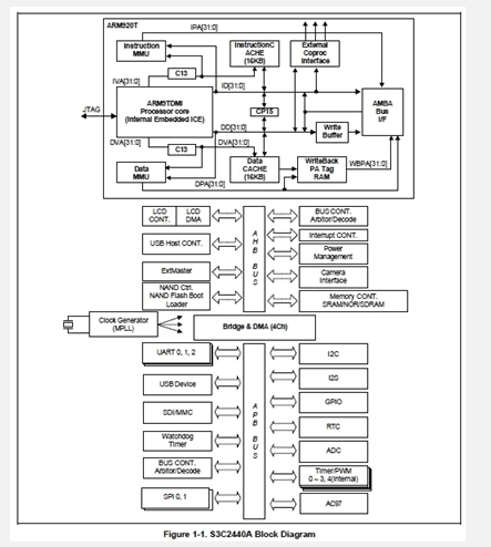
The SAMSUNG S3C2440A40-YQ80 16/32-bit RISC microprocessor is designed to provide hand-held devices and general applications with low-power, and high-performance microcontroller solution in small die size. The S3C2440A40-YQ80 is developed with ARM920T core, 0.13um CMOS standard cells and a memory complier. Its lowpower, simple, elegant and fully static design is particularly suitable for cost- and power-sensitive applications. It adopts a new bus architecture known as Advanced Micro controller Bus Architecture (AMBA). The S3C2440A40-YQ80 offers outstanding features with its CPU core, a 16/32-bit ARM920T RISC processor designed by Advanced RISC Machines, Ltd. The ARM920T implements MMU, AMBA BUS, and Harvard cache architecture with separate 16KB instruction and 16KB data caches, each with an 8-word line length.
Parametrics
S3C2440A40-YQ80 absolute maximum ratings: (1)VDDi: 1.2V VDD, 1.8 V; (2)VDDOP: 3.3V VDD, 4.8V; (3)VDDMOP: 1.8V/2.5V/3.0V/3.3V VDD, 4.8V; (4)VDDRTC: 1.8V/2.5V/3.0V/3.3V VDD, 4.5v; (5)VDDADC: 3.3V VDD, 4.8V; (6)DC Input Voltage, VIN: 3.3V Input buffer, 4.8v; 3.3V Interface / 5V Tolerant input buffer, 6.5v; (7)DC Output Voltage, VOUT: 3.3V Output buffer, 4.8v; (8)DC Input (Latch-up) Current, IIN:± 200 mA; (9)Storage Temperature, TSTG: – 65 to 150 ℃.
Features
S3C2440A40-YQ80 features: (1)Integrated system for hand-held devices and general embedded applications; (2)16/32-Bit RISC architecture and powerful instruction set with ARM920T CPU core; (3)Enhanced ARM architecture MMU to support WinCE, EPOC 32 and Linux; (4)Instruction cache, data cache, write buffer and Physical address TAG RAM to reduce the effect of main memory bandwidth and latency on performance; (5)ARM920T CPU core supports the ARM debug architecture; (6)Internal Advanced Microcontroller Bus Architecture (AMBA) (AMBA2.0, AHB/APB); (7)Little/Big Endian support; (8)Support Fast bus mode and Asynchronous bus mode; (9)Address space: 128M bytes for each bank (total 1G bytes); (10)Supports programmable 8/16/32-bit data bus width for each bank; (11)Fixed bank start address from bank 0 to bank 6; (12)Programmable bank start address and bank size for bank 7.
Diagrams

 |
 S3C2400 |
 Other |
 |
 Data Sheet |
 Negotiable |
|
||||
 |
 S3C2410A |
 Other |
 |
 Data Sheet |
 Negotiable |
|
||||
 |
 S3C2410X |
 Other |
 |
 Data Sheet |
 Negotiable |
|
||||
 |
 S3C2412XL-26 |
 Other |
 |
 Data Sheet |
 Negotiable |
|
||||
 |
 S3C2440A |
 Other |
 |
 Data Sheet |
 Negotiable |
|
||||
 |
 S3C2440A-40-YQ80 |
 Other |
 |
 Data Sheet |
 Negotiable |
|
||||
 (China (Mainland))


